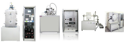
Wafer Contamination Scanner powerful, fully automated wafer metal-contaminant detection System
Vacuum technologies are the core fundamental covering
extensive industrial areas such as the space engineering, the biotechnology,
the material engineering and the chemical engineering. To respond various
demands for such fundamentals, we are producing/supplying various products from
small devices and large scaled equipment including vacuum devices for
researches, semiconductor testing devices, display process equipment, furnaces
for semiconductors and valves for chemical applications.
TDS (Thermal
Desorption Spectroscopy):
Thermal Desorption Spectroscopy (TDS) is mostly used to
acquire information on the biding energies of molecules and atoms. The quantity
and substance of a gas occurring in the vacuum process are analyzed by using
the vacuum gage and the mass spectrometer. This technology enables the
detection of the quantity change and the composition of a gas even in a minimal
amount and the measurements of temporal change of the gas in each temperature
in a vacuum device.
WCS (Wafer
Contamination Scanner):
Powerful, fully automated wafer metal-contaminant detection
System. Developed in collaboration with a major semiconductor Company.
Key characteristics
include the following:
·
Fully automated and equipped with EFEM,
automatic calibration for quantitative analysis
·
Patented scanning nozzle works on various wafer
surfaces including hydrophobic and hydrophilic surfaces, patterned wafer and
glasses.
·
Chemical supply system that automatically
residue removal, which improves safety.
·
Flexible scan mode (i.e. full, radial, sector,
chip mapping) and can be customized
·
Higher etching speed from its improved nebulizer
and spraying knife
WCS (Wafer
Contamination Scanner) M300:
WCS-M300 utilizes ICP-MS (Inductively Coupled Plasma Mass
Spectrometry) for further detecting and characterizing metal trace on wafer
surface. Agilent sensor used (others sensors can be adopted).
·
Inductively coupled plasma ionizes the sample.
·
Metal contaminant detection can detect down to
one part per trillion
·
Detection Limit-1X10⁷ atoms/cm2 on 300mm wafer
·
Survey Limit-over 60 elements in a single
survey.
Scanning:
ν Applicable wafer
materials
·
extended applicability to various materials by
patented scan nozzle system
·
very hydrophobic ~ hydrophilic surface
·
possible to scan patterned wafers and glasses
ν Scan mode
·
ull, radial, edge scan and point scan
·
wafer rotation & nozzle linear motion
Looking for wafer contamination
scanner manufacturer and Vacuum
technology based system? WCS (Wafer Contamination Scanner) powerful, fully
automated wafer metal-contaminant detection System. Developed in collaboration
with a major semiconductor Company. Higher etching speed from its improved
nebulizer and spraying knife.


Comments
Post a Comment